Lugansk Association of Radio Amateurs - output loop system. Cold tuning of the p-circuit Methods for turning on the output P-circuit
Transcript
1 392032, Tambov Aglodin G. A. P CONTOUR Features of the P circuit In the age of the victorious march of modern semiconductor technologies and integrated circuits, tube high-frequency power amplifiers have not lost their relevance. Tube power amplifiers, like transistor power amplifiers, have their own advantages and disadvantages. But the undeniable advantage of tube power amplifiers is that they operate on a mismatched load without failure of vacuum devices and without equipping the power amplifier with special mismatch protection circuits. An integral part of any tube power amplifier is the anode P circuit (Fig. 1). In the work r Methodology for calculating the P circuit of a transmitter, Konstantin Aleksandrovich Shulgin gave a very detailed and mathematically accurate analysis of the P circuit. Fig. 1 To save the reader from searching for the necessary journals (after all, more than 20 years have passed), below are the formulas for calculating the P circuit borrowed from: fo = f N f B (1) geometric mean frequency of the Hz range; Qn X r = loaded quality factor P of the circuit; the intrinsic quality factor P of the circuit is mainly determined by the quality factor of the inductive element and has a value within (in some sources it is designated as Q XX); own losses in the circuit, mainly in the inductor, cannot be accurately calculated, since it is necessary to take into account the skin effect and radiation losses along the field. The indicated formula has an error of ±20%; N = (2) transformation coefficient P of the circuit; equivalent resistance of the anode circuit of the power amplifier; load resistance (feeder line resistance, antenna input resistance, etc.); Qn η = 1 (3) P circuit efficiency;
2 X = N η η (Qn η) N 1 Qn (4); X X = Qn X η (5); Qn X X = (6); η 2 2 (+ X) 2 10 = X 10 = 6 12 pf (7); X µgn (9); 10 = 12 pf (8); The X P circuit, on the one hand, is a resonant circuit with a quality factor Qn, on the other hand, a resistance transformer that converts a low-resistance load resistance into a high-resistance equivalent resistance of the anode circuit. Let's consider the possibility of transforming, using a P circuit, different values of load resistance into the equivalent resistance of the anode circuit under the condition =const. Let's say it is necessary to implement a P circuit for a power amplifier assembled on four GU-50 pentodes connected in parallel according to a circuit with a common grid. The equivalent resistance of the anode circuit of such an amplifier will be = 1350 Ohm (for each pentode 5400 ± 200 Ohm), the output power will be approximately R OUT W, the power consumed from the power source R PO W. According to the given conditions: range 80 meters, fo = f f = = , N V =1350 Ohm, Qn=12, =200 using formulas (1) (9) we will calculate for five values: =10 Ohm, =20 Ohm, =50 Ohm , =125 Ohm, =250 Ohm. The calculation results are shown in Table 1. Table 1 range 80 meters, fo= Hz, =1350 Ohm, Qn=12, =200 SWR N pf μgn pf,78 5.7 20 2.5 67.5 357.97 5.8 50 1.0 27.0 333.04 6.5 10.8 302.98 7.94 972.4 273.80 9.56 642.2 Similar calculations must be made for other ranges. More clearly, the changes in the values of the elements and the load resistance are shown in the form of graphs as a function of Fig. 2.
3 400 C1 pf μg 8.8 7.2 5, pf Fig. 2 Let us note the characteristic features of the graphs: the value of capacitance C1 decreases monotonically, the value of inductance increases monotonically, but the value of capacitance C2 has a maximum at = 16 20 Ohms. This must be paid special attention to and taken into account when choosing the tuning range of capacitance C2. Moreover, the load resistance is of a purely active nature quite rarely; as a rule, the load (antenna) resistance is complex in nature and to compensate for the reactive component, an additional margin is required in the tuning range of the elements of the P circuit. But it is more correct to use an ACS unit (antenna matching device) or an antenna tuner. It is advisable to use ACS with tube transmitters; for transistor transmitters, ACS is mandatory. Based on the above, we come to the conclusion that in order to coordinate when the load resistance changes, it is necessary to rearrange all three elements of the P circuit in Fig. 3. Fig. 3 Practical implementation of the P circuit Since the mid-60s of the last century, the P circuit diagram Fig. 4 has been circulating, which seems to have taken root and does not arouse much suspicion. But let's pay attention to the method of switching the inductive element in the P circuit. 1 2 S Fig.4 T Fig.5 S Whoever tried to switch a transformer or autotransformer in a similar way, Fig.5. Even one short-circuited turn can lead to complete failure of the entire transformer. And with the inductor in the P circuit, without a shadow of a doubt, we do exactly the same!?
4 Firstly, the magnetic field of the open part of the inductor creates a short circuit current I SC in the closed part of the coil Fig. 6. For reference: the amplitude of the current in the P circuit (and in any other resonant system) is not so small: I K 1 A1 = I Qn = 0.8A, where: I K1 is the amplitude of the resonant current in the P circuit; I A1 amplitude of the first harmonic of the anode current (for four GU-50 I A1 0.65A) Fig. 6 And where will the energy of the short circuit current be spent (I short circuit Fig. 6): for heating the short-circuited turns themselves and for heating the contact nodes of the switch S (Fig. 4). Q-meter Fig. 7 Q-meter Q =200 Q Short circuit 20 a) b) Secondly, if it is possible to use a Q-meter (quality factor meter), take readings from an open inductor and with partially closed turns Fig. 7a, fig. 7b Q of the short circuit will be several times less than Q, now using formula (3) we determine the efficiency of the P circuit: Qn 12 η = 1 = 1 = 0.94, 200 Qn 12 η short circuit = 1 = 1 = 0.4?! kz 20 At the output of the P circuit we have 40% of the power, 60% went to heating, eddy currents, etc. Summarizing the first and second, we end up with not a P circuit, but some kind of RF crucible. I Short circuit What are the ways to constructively improve the P circuit: Option 1, the circuit according to Fig. 4 can be modernized as follows: the number of inductive elements should be equal to the number of ranges, and not two or three coils as usual. To reduce the magnetic interaction of nearby coils, their axes must be placed perpendicular to each other, at least in space there are three degrees of freedom, coordinates X, Y, Z. Switching is carried out at the junction of individual coils. Option 2: use tunable inductive elements, such as variometers. Variometers will allow you to more finely tune the P circuit (Table 1 and Fig. 3). Option 3: use a type of switching that excludes the presence of closed or partially closed coils. One of the possible options for the switching circuit is shown in Fig. 8.
5 M M M Fig. 8 Literature 1. Shulgin K. A. Methodology for calculating the P circuit of a Radio transmitter, 7
3.5. Complex parallel oscillatory circuit I A circuit in which at least one parallel branch contains reactivity of both signs. I C C I I There is no magnetic connection between and. Resonance condition
Antenna matching device Completed by: student gr. FRM-602-0 Purpose: Development of an automatic control circuit of the AnSU for its servo self-adjustment to a given IKB Tasks: 1) Study the design and principles
Problems in the discipline “Electronics” included in test 2 1. In a parallel oscillating circuit (see figure) at a resonant voltage U k0, active power P 0 is consumed.. Determine
Lecture Topic: oscillatory systems Isolation of a useful signal from a mixture of various side signals and noise is carried out by frequency-selective linear circuits, which are built on the basis of oscillatory
0. Pulse signal measurements. The need to measure the parameters of pulse signals arises when it is necessary to obtain a visual assessment of the signal in the form of oscillograms or readings from measuring instruments,
Complex amplitude method Harmonic voltage oscillations at the terminals of elements R or causes the flow of a harmonic current of the same frequency. Differentiation, integration and addition of functions
ANSWER SHEET Exercise 1.1.1. U U out in R 2 R 1 C 2 2 1 arctg RC Exercise 1.1.2. f, Hz U in, V U out, V, o s2 () s tg() 50.0 23.0 6.7 0.291 73.6 400.00 11.78 20.00 3.4 64.6 23, 0 8.4 0.365 66.9 240.37
Practical tasks for the exam in the discipline “Radio Engineering Circuits and Signals” 1. Free vibrations in an ideal circuit have a voltage amplitude of 20V, a current amplitude of 40mA and a wavelength of 100m. Define
RU9AJ "HF and VHF" 5 2001 Power amplifier based on GU-46 tubes The glass pentode GU-46 is becoming increasingly popular among shortwave operators, on which RU9AJ built a powerful amplifier for all amateur
The invention relates to electrical engineering and is intended for the implementation of powerful, cheap and efficient adjustable transistor high-frequency resonant voltage converters for various applications,
Practical lessons on thermal power plants. Task list. class. Calculation of equivalent resistances and other relationships.. For a circuit a c d f, find the equivalent resistances between terminals a and, c and d, d and f, if =
Ministry of Education and Science of the Russian Federation KAZAN NATIONAL RESEARCH TECHNICAL UNIVERSITY (KNITU-KAI) named after. A. N. TUPOLEVA Department of Radioelectronic and Quantum Devices (REKU) METHODOLOGICAL INSTRUCTIONS
33. Resonance phenomena in a series oscillatory circuit. Purpose of the work: Experimentally and theoretically investigate resonance phenomena in a series oscillatory circuit. Required equipment:
Lecture 8 Topic 8 Special amplifiers Direct current amplifiers Direct current amplifiers (DC amplifiers) or amplifiers of slowly varying signals are amplifiers that are capable of amplifying electrical
Moscow State University named after. M.V. Lomonosov Faculty of Physics Department of General Physics Laboratory practice in general physics (electricity and magnetism) Laboratory
3.. Forced oscillations in a series circuit Series and parallel circuits E I - the resistance of the circuit's own losses - the resistance of the signal source and - the load resistance
03090. Linear circuits with inductively coupled coils. Purpose of work: Theoretical and experimental studies of a circuit with mutual inductance, determination of the mutual inductance of two connected magnetic
LABORATORY WORK 3 STUDYING FORCED OSCILLATIONS IN AN OSCILLATING CIRCUIT Purpose of work: to study the dependence of the current strength in an oscillatory circuit on the frequency of the EMF source included in the circuit and measurement
RUSSIAN FEDERATION (19) RU (11) (51) IPC H03B 5/12 (2006.01) 173 338 (13) U1 R U 1 7 3 3 3 8 U 1 FEDERAL INTELLECTUAL PROPERTY SERVICE (12) DESCRIPTION OF THE UTILITY MODEL FOR THE PATENT (2 1 )(22)
DEVICE FOR COMPENSATION OF REACTIVE POWER IN AN ELECTRIC CIRCUIT The invention relates to the field of electrical engineering and is intended for use in industrial electrical networks of enterprises for compensation
Laboratory work “Bridge measurements” Measuring bridge A measuring bridge is an electrical device for measuring resistance, capacitance, inductance and other electrical quantities. Bridge
Laboratory work 6 Study of the phenomenon of self-induction. Purpose of the work: to investigate the features of the phenomenon of self-induction, measure the inductance of the coil and the EMF of self-induction. Equipment: coil 3600 turns R L»50
Lecture 7 Topic: Special amplifiers 1.1 Power amplifiers (output stages) Power amplification stages are usually output (final) stages to which an external load is connected, and are designed
Laboratory work 16 Transformer. Purpose of the work: to study the operation of the transformer in idle mode and under load. Equipment: transformer (assemble a circuit for a step-down transformer!), source
LABORATORY WORK 5 Electric circuits with mutual inductance 1. Work assignment 1.1. In preparation for work, study: , . 1.2. Study of inductively coupled circuits
Page 1 of 8 6P3S (output beam tetrode) The main dimensions of the 6P3S lamp. General data The 6PCS beam tetrode is designed to amplify low frequency power. Applicable in single-stroke and push-pull outputs
CONTENT OF THE ACADEMIC DISCIPLINE LIST AND CONTENT OF SECTIONS (MODULES) OF THE DISCIPLINE Discipline module Lectures, part-time 1 Introduction 0.25 2 Linear electrical circuits of direct current 0.5 3 Linear electrical
5.3. Complex resistance and conductivity. Complex resistance of the circuit impedance: x Ohm's law in complex form: i u i u e e e e e e i u i u The module is equal to the ratio of the voltage and current amplitudes a
Option 708 A source of sinusoidal EMF e(ωt) sin(ωt ψ) operates in an electrical circuit. The circuit diagram is shown in Fig. The effective value of the EMF E of the source, the initial phase and the value of the circuit parameters
Measuring the parameters of magnetic circuits using the resonant method. The resonance measurement method can be recommended for use in a home laboratory along with the voltmeter-ampmeter method. What makes him different is
Resonance “in the palm of your hand.” Resonance is the mode of a passive two-terminal network containing inductive and capacitive elements, in which its reactance is zero. Resonance condition
Download the operating instructions for the radio station r 140m >>> Download the operating instructions for the radio station r 140m Download the operating instructions for the radio station r 140m The circuits are connected to each other through
G. Gonchar (EW3LB) “HF and VHF” 7-96 Something about RA Most amateur radio stations use a structural diagram: a low-power transceiver plus RA. There are different RAs: GU-50x2(x3), G-811x4, GU-80x2B, GU-43Bx2
LABORATORY WORK 1 STUDY OF DC ENERGY TRANSFER FROM AN ACTIVE TWO-PORT TO LOAD Purpose of the work: To learn to determine the parameters of an active two-terminal network in various ways: using
The capacitor of the oscillating circuit is connected to a constant voltage source for a long time (see figure). At t = 0, switch K is moved from position 1 to position 2. Graphs A and B represent
PGUPS Laboratory work 21 “Study of an inductive coil without a core” Performed by V.A. Kruglov. Checked by Kostrominov A.A. St. Petersburg 2009 Contents Contents... 1 List of symbols:...
QUESTIONS OF INPUT CONTROL OF STUDENTS’ KNOWLEDGE IN THE DISCIPLINE “Transient processes in electric power systems” 1 2 I 1 2 V 1 1. = 80v, U = v 2. = 0v, U = 7 v 3. = 30v, U = v 8 2 Determine the value EMF
CHECK WORK Test is one of the forms of independent educational activity of students to use and deepen the knowledge and skills acquired in lectures, laboratory and practical courses.
CALCULATION OF THE OUTPUT TRANSFORMER RESISTANCE OF THE UHF TRANSMITTER Alexander Titov Home address: 634050, Russia, Tomsk, Lenin Ave., 46, apt. 28. Tel. 51-65-05, E-mail: [email protected](Circuit design.
Electrical Engineering Test. Option 1. 1.What devices are shown in the diagram? a) a light bulb and a resistor; b) light bulb and fuse; c) a source of electric current and a resistor.
5.12. INTEGRAL AC VOLTAGE AMPLIFIERS Low frequency amplifiers. ULF in an integrated design is, as a rule, aperiodic amplifiers covered by a common (direct and alternating current)
Broadband transformers, 50-ohm units, have circuits inside them with a resistance that is often significantly different from 50 ohms and lies in the range of 1-500 ohms. In addition, it is necessary that the input/output of a 50-ohm
Examples of possible schemes for solving problems of a semester assignment Assignment. Methods for calculating linear electrical circuits. The task. Determine the current flowing in the diagonal of an unbalanced Wheatstone bridge
Laboratory work 4 ELECTRICAL OSCILLATING CIRCUIT Purpose of the work To study the theory of resonant radio circuits of oscillatory circuits (series and parallel). Explore the frequency response and phase response
050101. Single-phase transformer. Purpose of work: To become familiar with the device and operating principle of a single-phase transformer. Remove its main characteristics. Required equipment: Modular training complex
LABORATORY WORK Amplitude modulator Purpose of the work: to investigate a method for obtaining an amplitude-modulated signal using a semiconductor diode. Controlling the amplitude of high-frequency oscillations
Ministry of Education and Science of the Russian Federation Kazan National Research Technical University named after. A.N.Tupoleva (KNRTU-KAI) Department of Radioelectronic and Quantum Devices (REKU) Guidelines
Sinusoidal current “in the palm of your hand” Most of the electrical energy is generated in the form of EMF, which changes over time according to the law of a harmonic (sinusoidal) function. The sources of harmonic EMF are
Laboratory work 6 Study of the local oscillator board of a professional receiver Purpose of the work: 1. To become familiar with the circuit diagram and design of the local oscillator board. 2. Remove the main characteristics
Methods for including a transistor in an amplifier stage circuit As mentioned in Section 6, the amplifier stage can be represented by a 4-pole network to the input terminals of which a signal source is connected
State educational institution of secondary vocational education "Novokuznetsk College of Food Industry" WORK PROGRAM OF THE ACADEMIC DISCIPLINE Electrical and electronic engineering
03001. Elements of electrical circuits of sinusoidal current Purpose of work: To become familiar with the basic elements of electrical circuits of sinusoidal current. Master the methods of electrical measurements in sinusoidal circuits
Electromagnetic oscillations Quasi-stationary currents Processes in an oscillatory circuit An oscillatory circuit is a circuit consisting of an inductor, capacitor C and a resistor connected in series
LABORATORY WORK ON THE THEORETICAL FUNDAMENTALS OF ELECTRICAL ENGINEERING Contents: ORDER OF PERFORMANCE AND REGISTRATION OF LABORATORY WORK... 2 MEASURING INSTRUMENTS FOR PERFORMING LABORATORY WORK... 2 WORK 1. LAWS
11. Theorem about equivalent source. A is an active two-terminal network, - an external circuit. There is no magnetic connection between parts A and. A I A U U XX A I Short circuit 1. Theorem on the equivalent voltage source (Thevenin’s theorem):
Mordovian State University named after N.P. Ogarev Institute of Physics and Chemistry Department of Radio Engineering Bardin V.M. RADIO TRANSMITTER DEVICES, POWER AMPLIFIERS AND TERMINAL CASCADES OF RADIO TRANSMITTERS. Saransk,
Coils and transformers with steel cores Basic provisions and relationships. A steel circuit is an electrical circuit whose magnetic flux is completely or partially contained in one
Part 1. Linear DC circuits. Calculation of a DC electrical circuit using the folding method (equivalent replacement method) 1. Theoretical questions 1.1.1 Give definitions and explain the differences:
58 A. A. Titov UDC 621.375.026 A. A. TITOV PROTECTION OF BANDPASS POWER AMPLIFIERS FROM OVERLOADS AND MODULATION OF THE AMPLITUDE OF POWER SIGNALS It is shown that a bipolar transistor is a controlled limiter
3.4. Electromagnetic oscillations Basic laws and formulas Own electromagnetic oscillations arise in an electrical circuit, which is called an oscillatory circuit. Closed oscillatory circuit
PREFACE CHAPTER 1. DC CIRCUITS 1.1. Electric circuit 1.2. Electric current 1.3. Resistance and conductivity 1.4. Electric voltage. Ohm's law 1.5. Relationship between EMF and source voltage.
Page 1 of 8 The automatic antenna tuner of the proprietary transceiver completely refuses to match the input of the good old PA on a lamp with a common grid. But the old homemade apparatus was agreed upon and
List of topics in the program of the subject “Electrical Engineering” 1. DC electrical circuits. 2. Electromagnetism. 3. AC electrical circuits. 4. Transformers. 5. Electronic devices and instruments.
(c.1) Test questions on “Electronics”. Part 1 1. Kirchhoff's first law establishes the connection between: 1. Voltage drops across elements in a closed circuit; 2. Currents in the circuit node; 3. Power dissipation
Topic 11 RADIO RECEIVER DEVICES Radio receivers are designed to receive information transmitted via electromagnetic waves and convert it to a form in which it can be used
LABORATORY WORK 6 Study of an air transformer. Work assignment.. In preparation for work, study:, ... Construction of an equivalent circuit for an air transformer..3.
\main\r.l. designs\power amplifiers\... Power amplifier on the GU-81M based on the PA from R-140 Brief technical characteristics of the amplifier: Uanode.. +3200 V; Uc2.. +950 V; Uc1-300 V (TX), -380 V (RX);
Work 1.3. Studying the phenomenon of mutual induction Purpose of the work: studying the phenomena of mutual induction of two coaxially located coils. Instruments and equipment: power supply; electronic oscilloscope;
LABORATORY WORK 1 RESEARCH OF A BROADBAND TRANSFORMER Objectives of the work: 1. Study of the operation of a transformer in the frequency range under harmonic and impulse influences. 2. Study of the main
1 option A1. In the equation of harmonic vibration q = qmcos(ωt + φ0), the quantity under the cosine sign is called 3) the amplitude of the charge A2. The figure shows a graph of the current strength in a metal
Topic 9. Characteristics, starting and reversing of asynchronous motors. Single-phase asynchronous motors. Topic questions.. Asynchronous motor with wound rotor.. Performance characteristics of an asynchronous motor. 3.
Place of the discipline in the structure of the educational program The discipline “Fundamentals of Electrical Engineering and Electronics” is a discipline of the basic part. The work program is drawn up in accordance with the requirements of the Federal
Let's continue the conversation about the features that any radio amateur faces when designing a powerful RA amplifier and the consequences that can occur if the amplifier structure is installed incorrectly. This article provides only the most necessary information that you need to know and take into account when independently designing and manufacturing high-power amplifiers. The rest will have to be learned from your own experience. There is nothing more valuable than your own experience.
Cooling the output stage
The cooling of the generator lamp must be sufficient. What does this mean? Structurally, the lamp is installed in such a way that the entire flow of cooling air passes through its radiator. Its volume must correspond to the passport data. Most amateur transmitters are operated in the “receive-transmit” mode, so the volume of air indicated in the passport can be changed in accordance with the operating modes.
For example, you can enter three fan speed modes:
- maximum for contest work,
- average for everyday use and minimal for DX work.
It is advisable to use low noise fans. It is appropriate to recall that the fan turns on simultaneously with the filament voltage turning on or a little earlier, and turns off no less than 5 minutes after it is removed. Failure to comply with this requirement will shorten the life of the generator lamp. It is advisable to install an aero switch along the path of the air flow, which, through the protection system, will turn off all supply voltages in the event of a loss of air flow.
In parallel with the fan supply voltage, it is useful to install a small battery as a buffer, which will support the fan operation for several minutes in the event of a power failure. Therefore, it is better to use a low voltage DC fan. Otherwise, you will have to resort to the option I heard on the air from one radio amateur. He, supposedly to blow the lamp in the event of a power outage, keeps in the attic a huge inflated chamber from the rear wheel of the tractor, connected to the amplifier by an air hose.
Amplifier anode circuits
In high-power amplifiers, it is advisable to get rid of the anode choke by using a series power supply circuit. The apparent inconvenience will more than pay off with stable and highly efficient operation on all amateur bands, including ten meters. True, in this case the output oscillating circuit and the range switch are under high voltage. Therefore, variable capacitors should be decoupled from the presence of high voltage on them, as shown in Fig. 1.
Fig.1.
The presence of an anode choke, if its design is unsuccessful, can also cause the above phenomena. As a rule, a well-designed amplifier using a series-powered circuit does not require the introduction of “antiparaeits” either in the anode or in the grid circuits. It works stably on all ranges.
Separating capacitors C1 and C3, Fig. 2 must be designed for a voltage 2...3 times higher than the anode voltage and sufficient reactive power, which is calculated as the product of the high-frequency current passing through the capacitor and the voltage drop across it. They can be composed of several parallel-connected capacitors. In the P-circuit, it is advisable to use a variable-capacity vacuum capacitor C2 with a minimum initial capacitance, with an operating voltage no less than the anode one. Capacitor C4 must have a gap between the plates of at least 0.5 mm.
The oscillatory system, as a rule, consists of two coils. One for high frequencies, the other for low frequencies. The HF coil is frameless. It is wound with a copper tube with a diameter of 8...9 mm and has a diameter of 60...70 mm. To prevent the tube from becoming deformed during winding, fine dry sand is first poured into it and the ends are flattened. After winding, cutting off the ends of the tube, the sand is poured out. The coil for the low frequency ranges is wound on a frame or without it with a copper tube or thick copper wire with a diameter of 4...5 mm. Its diameter is 80...90 mm. During installation, the coils are positioned mutually perpendicular.
Knowing the inductance, the number of turns for each range, can be calculated with high accuracy using the formula:
L (μH) = (0.01DW 2)/(l/ D + 0.44)
However, for convenience, this formula can be presented in a more convenient form:
W= C (L(l/ D + 0.44))/ 0.01 - D; Where:
- W is the number of turns;
- L - inductance in microhenry;
- I - winding length in centimeters;
- D is the average diameter of the coil in centimeters.
The diameter and length of the coil are set based on design considerations, and the inductance value is selected depending on the load resistance of the lamp used - table 1.
Table 1.
Variable capacitor C2 at the “hot end” of the P-circuit, Fig. 1, is connected not to the anode of the lamp, but through a tap of 2...2.5 turns. This will reduce the initial loop capacitance on the HF bands, especially on 10 meters. The taps from the coil are made with copper strips 0.3...0.5 mm thick and 8...10 mm wide. First, they need to be mechanically secured to the coil by bending a strip around the tube and tightened with a 3 mm screw, having previously tinned the connection and outlet points. Then the contact point is carefully soldered.
Attention: When assembling powerful amplifiers, you should not neglect good mechanical connections and rely only on soldering. We must remember that during operation all parts become very hot.
It is not advisable to make separate taps for WARC bands in coils. As experience shows, the P-circuit is perfectly tuned on the 24 MHz range in the 28 MHz switch position, on 18 MHz in the 21 MHz position, on 10 MHz in the 7 MHz position, with virtually no loss of output power.
Antenna switching
To switch the antenna in the “receive-transmit” mode, a vacuum or ordinary relay is used, designed for the appropriate switching current. To avoid burning the contacts, it is necessary to turn on the antenna relay for transmission before the RF signal is supplied, and for reception a little later. One of the delay circuits is shown in Fig. 2.
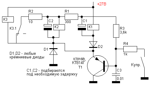
Fig.2.
When the amplifier is turned on for transmission, transistor T1 opens. Antenna relay K1 operates instantly, and input relay K2 will operate only after charging capacitor C2 through resistor R1. When switching to reception, relay K2 will turn off instantly, since its winding, together with the delay capacitor, is blocked by the contacts of relay K3 through the spark-extinguishing resistor R2.
Relay K1 will operate with a delay, which depends on the capacitance value of capacitor C1 and the resistance of the relay winding. Transistor T1 is used as a switch to reduce the current passing through the control contacts of the relay located in the transceiver.

Fig.3.
The capacitance of capacitors C1 and C2, depending on the turnips used, is selected within the range of 20...100 μF. The presence of a delay in the operation of one relay in relation to another can be easily checked by assembling a simple circuit with two neon bulbs. It is known that gas-discharge devices have an ignition potential higher than the combustion potential.
Knowing this circumstance, the contacts of relay K1 or K2 (Fig. 3), in the circuit of which the neon light will light up, will close earlier. Another neon will not be able to light up due to its reduced potential. In the same way, you can check the order of operation of the relay contacts when switching to reception by connecting them to the test circuit.
Summarize
When using lamps connected according to a common cathode circuit and operating without grid currents, such as GU-43B, GU-74B, etc., it is advisable to install a powerful 50 Ohm non-induction resistor with a power of 30...50 W at the input (R4 in Fig. 4).
- Firstly, this resistor will be the optimal load for the transceiver on all bands
- Secondly, it contributes to exceptionally stable operation of the amplifier without the use of additional measures.
To fully drive the transceiver, a power of several or tens of watts is required, which will be dissipated by this resistor.

Fig.4.
Safety precautions
It is useful to remind you about observing safety precautions when working with high-power amplifiers. Do not carry out any work or measurements inside the housing when the supply voltage is turned on or without making sure that the filter and blocking capacitors are completely discharged. If, if accidentally exposed to a voltage of 1000...1200V, there is still a chance to miraculously survive, then when exposed to a voltage of 3000V and above, there is practically no such chance.
Whether you like it or not, you should definitely provide for automatic blocking of all supply voltages when opening the amplifier case. When performing any work with a powerful amplifier, you must always remember that you are working with a high-risk device!
S. Safonov, (4Х1IM)
L. Evteeva
"Radio" No. 2 1981
The output P-circuit of the transmitter requires careful adjustment, regardless of whether its parameters were obtained by calculation or it was manufactured according to the description in the magazine. It must be remembered that the purpose of such an operation is not only to actually tune the P-circuit to a given frequency, but also to match it with the output impedance of the final stage of the transmitter and the characteristic impedance of the antenna feed line.
Some inexperienced radio amateurs believe that it is enough to tune the circuit to a given frequency only by changing the capacitances of the input and output variable capacitors. But in this way it is not always possible to obtain optimal matching of the circuit with the lamp and antenna.
The correct setting of the P-circuit can only be obtained by selecting the optimal parameters of all three of its elements.
It is convenient to configure the P-circuit in a “cold” state (without connecting power to the transmitter), using its ability to transform resistance in any direction. To do this, connect a load resistance R1 parallel to the input of the circuit, equal to the equivalent output resistance of the final stage Roe, and a high-frequency voltmeter P1 with a small input capacitance, and a signal generator G1 is connected to the output of the P-circuit - for example, in the antenna socket X1. Resistor R2 with a resistance of 75 Ohms simulates the characteristic impedance of the feeder line. 
The load resistance value is determined by the formula
Roe = 0.53Upit/Io
where Upit is the supply voltage of the anode circuit of the final stage of the transmitter, V;
Iо is the constant component of the anode current of the final stage, A.
The load resistance can be made up of BC type resistors. It is not recommended to use MLT resistors, since at frequencies above 10 MHz high-resistance resistors of this type exhibit a noticeable dependence of their resistance on frequency.
The process of “cold” tuning of the P-circuit is as follows. Having set the given frequency on the generator scale and introduced the capacitances of capacitors C1 and C2 to approximately one-third of their maximum values, according to the voltmeter readings, the P-circuit is tuned to resonance by changing the inductance, for example, by selecting the tap location on the coil. After this, by rotating the knobs of capacitor C1 and then capacitor C2, you need to achieve a further increase in the voltmeter reading and again adjust the circuit by changing the inductance. These operations must be repeated several times.
As you approach the optimal setting, changes in capacitor capacitances will affect the voltmeter readings to a lesser extent. When a further change in capacitances C1 and C2 will reduce the voltmeter readings, the adjustment of the capacitances should be stopped and the P-circuit should be adjusted as accurately as possible to resonance by changing the inductance. At this point, setting up the P-circuit can be considered complete. In this case, the capacitance of capacitor C2 should be used by approximately half, which will make it possible to correct the circuit settings when connecting a real antenna. The fact is that often antennas made according to the descriptions will not be tuned accurately. In this case, the conditions for mounting the antenna may differ markedly from those given in the description. In such cases, resonance will occur at a random frequency, a standing wave will appear in the antenna feeder, and a reactive component will be present at the end of the feeder connected to the P-circuit. It is for these reasons that it is necessary to have a reserve for adjusting the elements of the P-circuit, mainly capacitance C2 and inductance L1. Therefore, when connecting a real antenna to the P-circuit, additional adjustments should be made with capacitor C2 and inductance L1.
Using the described method, the P-circuits of several transmitters operating on different antennas were configured. When using antennas that were sufficiently well tuned to resonance and matched with the feeder, no additional adjustment was required.
Automatic adjustment of the anode capacitor of the P-circuit of the HF power amplifier
Principle of operation.
The theoretical basis for the development and manufacture of this device is the principle of comparing the voltage phases on the grid and on the anode of the lamp. It is known that at the moment of full resonance of the P-circuit, the phase difference between the voltages on the grid and the anode is strictly 180 degrees and the resistance of the anode load is purely active. A P-circuit that is not tuned to resonance has a complex resistance and, accordingly, a phase shift of the grid and anode voltages different from 180 degrees. The nature of the reactive component of the complex resistance depends on whether the natural resonance of the P-circuit is higher or lower in frequency relative to the operating frequency. Those. the capacitance of the capacitor on the anode side is greater or less relative to the capacitance at resonance.
Of course, the setting of the P-circuit is affected not only by the capacitance of the capacitor on the anode side, but this device does not pretend to fully automate the setting. That. the task is to rotate the capacitor axis to a position in which the reactive component of the complex resistance will be minimized in the event of a P-circuit detuning.
A similar problem was solved by Yu. Dailidov EW2AAA, using in his design a phase detector made according to a ring balanced circuit on diodes. The disadvantage of this scheme is the low accuracy of tuning, the need to select parts for a balanced mixer, the need for careful shielding, and as a result, a very strong frequency dependence and complexity of tuning.
That. this design can be considered as a modernization of the EW2AAA circuit design.
Design feature.
In this design, the phase detector is made on a digital chip DD2 type KR1531TM2. The operating principle is very simple and is based on the D-trigger operating algorithm, i.e. recording the state at input D along the leading edge of the pulse at input C. The logic elements NOT of the DD1 microcircuit act as shapers of rectangular pulses from the sinusoidal voltage on the grid and anode. That. A sequence of pulses is received at the inputs D and C of the flip-flops and their edges are compared.
For example, the voltage at the anode is ahead of the voltage at the grid, the edge of the positive pulse at input D of element DD3:1 appears earlier than the edge at input C, a unit is written and output 5 is set to “1”. At inputs D and C of element DD3:2, pulses appear exactly the opposite and, accordingly, zero “0” is recorded at output 9. If the phase of the voltage on the anode lags behind the phase of the voltage on the grid, the state of outputs 5 and 9 of the DD3 microcircuit changes to the opposite.
It should be noted that the moment of switching triggers from one state to another when the phase difference passes through 180 degrees is not ideal and has a certain “fork”, the width of which is determined by the delay time of the logic element and for 1531 series microcircuits is several nanoseconds. This “fork” mainly determines the maximum accuracy of tuning the P-circuit to resonance. Looking ahead, I note that the maximum accuracy of tuning tracking on the 14 MHz range is +- 5 KHz. What actually looks like rotating the anode capacitor tuning knob following the rotation of the transceiver frequency tuning knob.
Purpose of some elements of the circuit.
Capacitors C1 and C2 constitute a capacitive RF voltage divider of the anode. Capacitors C3 and C4 constitute a capacitive divider of the RF grid voltage.
The RF voltage taken from the dividers should be about 6 V in amplitude in operating mode. C1 – type KVI-1. C2 and C4 are passable.
Microcircuits DD2 and DD4 are integrated stabilizers; they may be absent if there is a separate +5V power supply.
DD5 - logical elements 3I - prevent the simultaneous appearance of logical ones at the output of the phase detector (which is unacceptable), and also block the operation of automatic tuning, if necessary, when closing the “Control” contacts.
The analog part of the circuit on transistors VT1-VT8 acts as a current amplifier with motor control switches and changes the polarity on the motor depending on the state of the logical one and zero at the output of the phase detector.
Transistors must have the letter B or G.
The “To LEDs” outputs can be used as a visual indication of the state of the phase detector (setting) when manually tuning to resonance.
Features of setup and installation.
All elements of the circuit are located on a printed circuit board in the basement of the chassis with the exception of C1, C2, C3, C4, R1, R2. No additional shielding of the printed circuit board is required.
From the capacitive dividers to the board, the signal is supplied via a shielded wire (cable). It is very important that the length of the cable from the divider C3, C4 must be greater than the length of the cable from the divider C1, C2. This is determined by the need to compensate for the signal delay in the lamp from the grid to the anode. In practice, the difference in length for the GU-43B lamp is 10 cm. In your particular case, the difference may be different.
It is interesting to note that the “fork” of tuning accuracy depends on the bias voltage on the DD1 elements. The bias voltage is selected using potentiometers R4 and R6 and in my case has the following dependence.
|
U bias on inputs 1 and 13 (V) |
Operation accuracy +-(KHz) |
That. it is necessary to set the voltage at the inputs of the microcircuits to 1.4 V, which ensures maximum adjustment accuracy.
The placement of the motor and its articulation with the axis of the tuning capacitor is not considered in this case because this is very individual and depends primarily on the capabilities of the designer. In my case, I use a motor with a gearbox from a money counting machine with an operating voltage of 6V. Therefore, it was necessary to install a limiting resistor with a nominal value of 62 Ohms in series with the motor. A vacuum capacitor KP1-8 5-250 pF is used as a tuning capacitor. The transmission of rotation is carried out through plastic gears.
It is advisable to use resistors of type C2-10 (non-inductive) as resistors R1 and R2, but this is not necessary.
- Download the complete set of files.
If you carefully look at the photograph of the printed circuit board, you will notice that instead of the KR1531LI3 microcircuit there is KR1531LI1. It’s just that the same logic can be performed on different elements; it’s easier on LI3, but I had LI1 on hand.
I am ready to provide all possible advisory assistance only by email: rv3fn()mail.ru
Mashukov Alexander Yurievich (RV3FN).
Automatic adjustment of the coupling capacitor of the P-circuit of the HF power amplifier
(addition to the article on automatic adjustment of the anode capacitor of the P-circuit)
Introduction
The P-circuit is a matching device between the active amplifying element (lamp or transistor) and the radiating device (antenna-feeder system). With rare exceptions, the resistances of these elements are different. In addition, their resistance is complex, i.e. In addition to the active, it has a reactive (capacitive or inductive) component.
Strictly speaking, both capacitances of the P-circuit affect both the tuning of the P-circuit to resonance and the degree of connection with the load (antenna). In the case of a tube amplifier, i.e. when the output resistance of the amplifying element is significantly greater than the resistance of the antenna, the influence of the capacitance of capacitor C1 has a greater effect on the resonance, and the influence of the capacitance of capacitor C2 on the level of communication with the antenna. We assume that C1 tunes the P-circuit to resonance, and C2 establishes the optimal level of communication with the antenna.
The indicator of the optimal communication level for a tetrode is the value of the screen grid current. This value is different for different lamps. Without going deeply into theory, I will only note that with an optimal screen grid current, the optimal level of unwanted harmonics in the spectrum of the emitted signal of a given power is ensured. In practice, during the setup process, by rotating the knob of capacitor C2, we set the desired screen grid current. So, it is necessary to automate this process.
Structural scheme

The current control unit of the second grid produces a signal when the current drops to a level of less than 20 mA and when the current is more than 40 mA. When the current is in the range of 20-40 mA, no signals are issued. Of course, the levels can change as desired during setup.
The control unit performs two functions. The first is to form a logic level for digital control of logic elements, the second is permission for motor control. That is, the motor can rotate (be controlled) only if there is a resonance condition in the P-circuit. This signal comes from the control unit for capacitor C1. And only if there is a required level of RF voltage at the anode. This is done in order to eliminate false rotation of the motor in the absence of a drive signal, when the screen grid current is zero, or when the current is too low due to insufficient drive.
The DC amplifier doesn't need much explanation. It is similar to the amplifier in the control circuit for capacitor C1, only it is made with different elements.
Schematic diagram

It should be noted here that in the previous article on setting up an anode capacitor, output to this circuit was not yet provided. Therefore, I present an upgraded anode capacitor control circuit. There are no fundamental changes in it. Only some parts have been replaced, signals for resonance control (A, B) have been removed, and a “Receive-Transmit” control signal has been added to prevent rotation of the motors in the (Receive) mode. This is the same control signal that comes from the transceiver to put the amplifier into transmit mode. In practice, with the correct setup of the circuit, such rotations do not occur, but during the setup process they are possible. This is like an additional guarantee. But let's return to our diagram.
R 6 and R 8 are shunt resistors through which the current of the second grid passes and on which the necessary voltage is actually released to open the diodes of the optocoupler DD 2. At a low current of the second grid (0-20mA), both LEDs are closed and the resistance of the output transistors of the optocoupler is high. At outputs 6 and 7 of the optocoupler there is a high voltage “1”. At normal current (20-40mA), one optocoupler opens, at a current of more than 40mA, the second optocoupler opens. Thus we have three modes. Up to 20mA, the motor should rotate in one direction, increasing the current of the second grid. The motor should be running in the current range of 20-40 mA. When the current is more than 40 mA, rotate in the other direction, reducing the current of the second grid. All this should work only at resonance, for which elements DD 1.2 and DD 1.1 are responsible, and only if there is a sufficient level of RF voltage at the anode of the lamp, for which the circuit on diodes VD 1, VD 2 and transistor VT 1 is responsible. Resistor R 1 sets the required the level of this voltage. At output 13 of element DD 1.4, the enabling logical “1” is set with “zeros” at inputs 11 and 12, i.e. when the above conditions are met. Elements DD 1.3 and DD 3.5 form the necessary coordination with the setting indication LEDs VD 4 and VD 5. Elements DD 4.1 and DD 4.2 generate control signals for the DC amplifier and analyze the presence of enabling signals, including the “manual - automatic” mode. DD 3.4 in manual mode supplies the required voltage to the manual engine rotation buttons KN 1 and KN 2; in automatic mode the buttons do not work. Buttons KN 3 and KN 4 limit switches are located on capacitor C2 in order to prevent its breakdown and protect the motor and circuit from excessive current in the event of the motor jamming at the edges of the rotation of the capacitor. The current amplifier is made on an opto-relay DD 5 and DD 6. Unlike the previous UPT circuit on transistors, this circuit provides greater reliability (the voltage drop on field-effect transistors is much lower) and of course is much simpler. The guarantee that the transistors will not be open simultaneously is provided by the back-to-back connection of the control diodes. Transistor VT 2 protects the optocoupler LEDs from excessive current. With a resistance of resistor R 11 of 8.2 Ohms, VT 2 opens at a current of about 65 mA. Diode VD3 protects the circuit from reverse currents.
Schematic diagram of anode capacitor control

Conclusion
The setup process can be sequential, i.e. with a smooth increase in the level of build-up or fast. I use fast. This is when the capacitor handles are placed in an approximate position for a given range, the transceiver output power regulator is set to the operating level, the transceiver is switched to AM mode and the pedal is pressed. First, the handle of capacitor C1 begins to rotate until resonance is established, then the motor of capacitor C2 is turned on and the desired current of the second grid is set. In this case, capacitor C2 sometimes stops and the resonance is corrected by capacitor C1. Sometimes you have to adjust the drive level to get the required power.
That's all. We switch the transceiver to SSB mode and do not forget to switch the switches to manual setting mode in order to avoid “yaw” of the capacitors during operation.
Good luck! Constructive comments are welcome.
R 3FN ex RV 3FN Alexander Mashukov.